


1

1
Very low quiescent current
n Output current in excess of 100 mA
n Input-output differential less than 0.6V
n Reverse battery protection
n 60V load dump protection
n −50V reverse transient protection
n Short circuit protection
n Internal thermal overload protection
n Mirror-image insertion protection
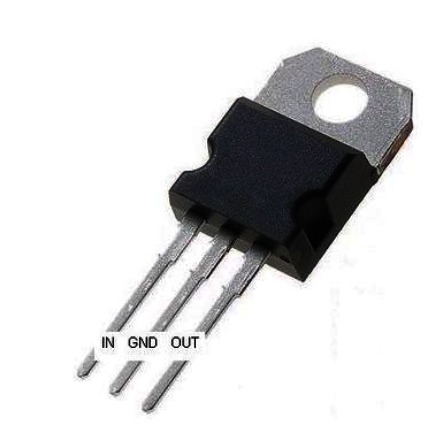
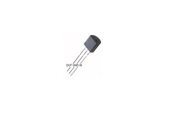
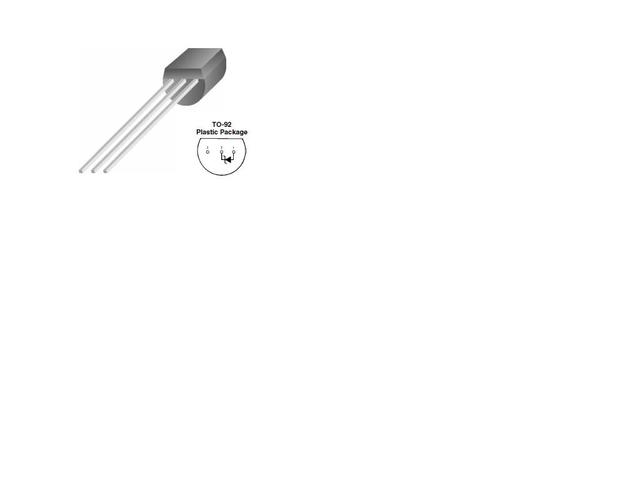
n Available in TO-220, TO-92, TO-263, SO-8 or 6-Bump
micro SMD packages
n Available as adjustable with TTL compatible switch
n See AN-1112 for micro SMD considerations

1
ア20 mV (ア0.8%) max. initial tolerance (A grade)
■ Operating current of 20 μA to 20 mA
■ 0.6Ω dynamic impedance (A grade)
■ Low temperature coefficient
■ Low voltage reference—1.2V
1
ア20 mV (ア0.8%) max. initial tolerance (A grade)
■ Operating current of 20 μA to 20 mA
■ 0.6Ω dynamic impedance (A grade)
■ Low temperature coefficient
■ Low voltage reference—2.5V
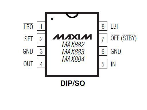
1
Guaranteed 200mA Output Current at
TJ = +125°C, with Foldback Current Limiting
High-Power (1.5W) 8-Pin SO Package
Dual Mode Operation: Fixed or Adjustable
Output from 1.25V to 11V
Large Input Range (2.7V to 11.5V)
Internal 1.1Ω P-Channel Pass Transistor
Draws No Base Current
Low 220mV Dropout Voltage at 200mA
Output Current
11μA (typ) Quiescent Current
1μA (max) Shutdown Mode or 7μA (typ)
Standby Mode
Low-Battery Detection Comparator
Reverse-Current Protection
Thermal-Overload Protection